The w11a CPU core
The w11a CPU core has a functionality very close to a PDP-11/70 CPU (Model KB11-B or KB11-C) and supports with very few exceptions everything the PDP-11 architecture has to offer:
- standard and extended (MUL, DIV, XOR, ASH) instruction set
- special instructions (SPL, MTPD, etc)
- dual register set
- three processor modes: kernel, supervisor, user
- memory management with 18 and 22 bit addressing and separate instruction and data address space
- UNIBUS mapping support (18->22 bit address translation)
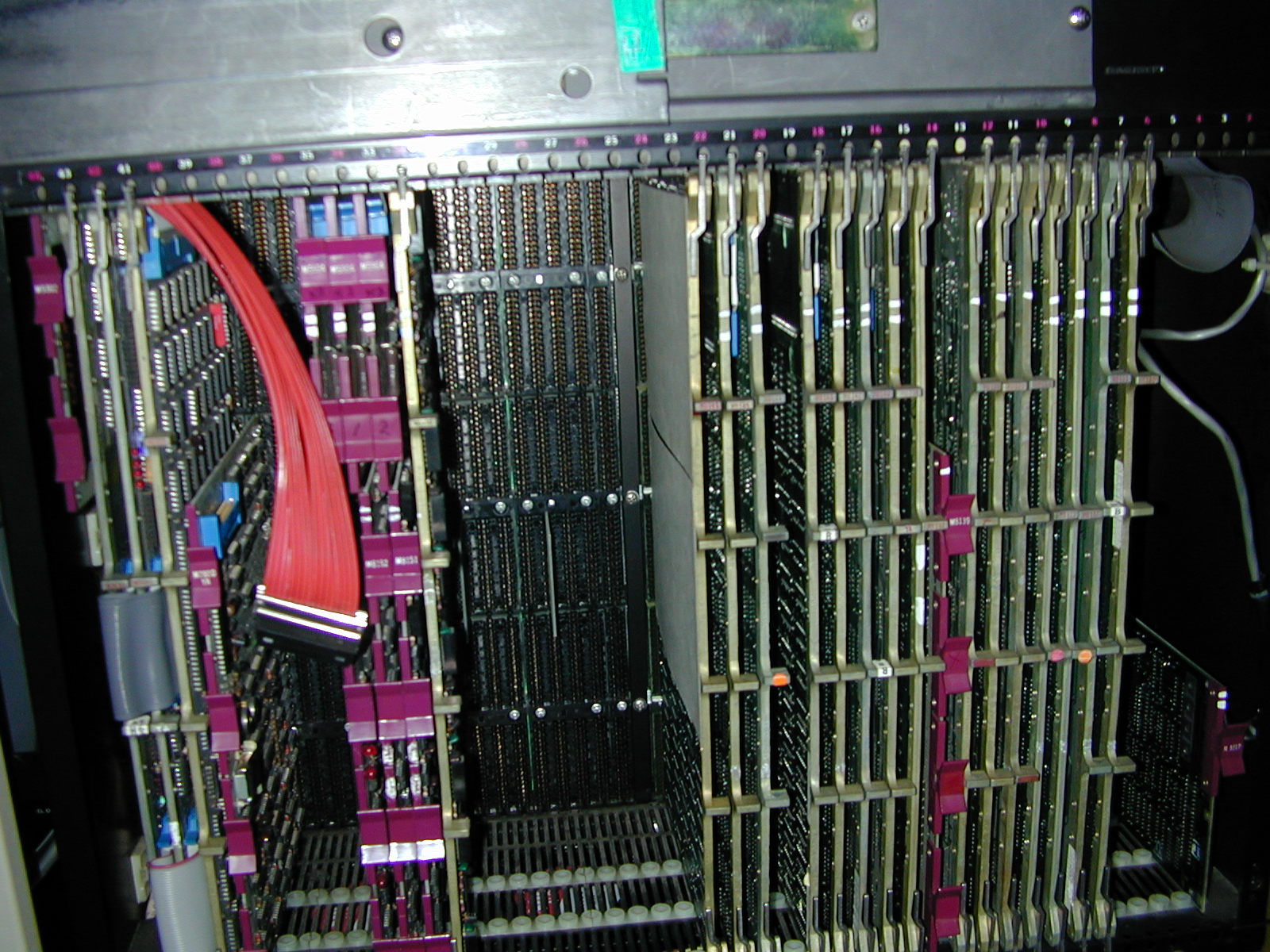
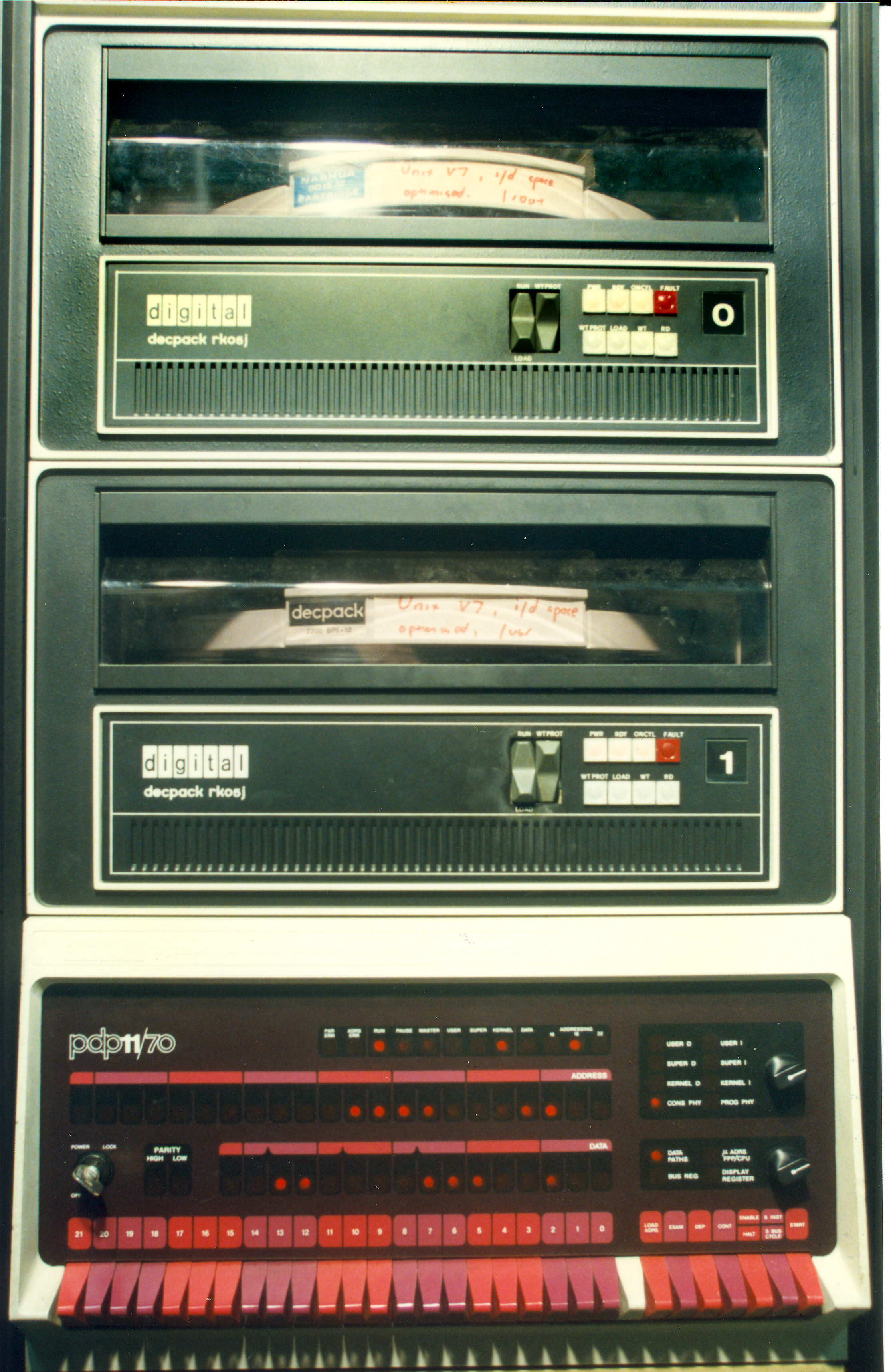
All fits today easily in a fraction of a modest size low-cost FPGA. The original 11/70 CPU was implemented in TTL, see Figure F-1 for comparison.
The I/O System
The project goal was to create a retro-computing platform able to run the historical UNIX systems and other original software. The I/O system is, therefore, set up to have the same register model and semantics as the original DEC UNIBUS peripherals. To interface this to contemporary I/O hardware all I/O transactions are emulated by a backend server in the following way:
- all device registers are effectively dual-ported, visible from the w11a core via a bus structure named ibus with an addressing model similar to the DEC UNIBUS, and from the backend server via a 'remote register interface', called rri.
- the rri communication between FPGA and backend server can be done directly via bus structure named rbus or over any bi-directional byte stream connection via the rlink protocol.
- an attention mechanism allows the efficient detection of significant device register state changes by the server, which will usually read the device state, emulate the desired I/O transaction and update the device state. DMA transfers are emulated by direct memory access over rbus.
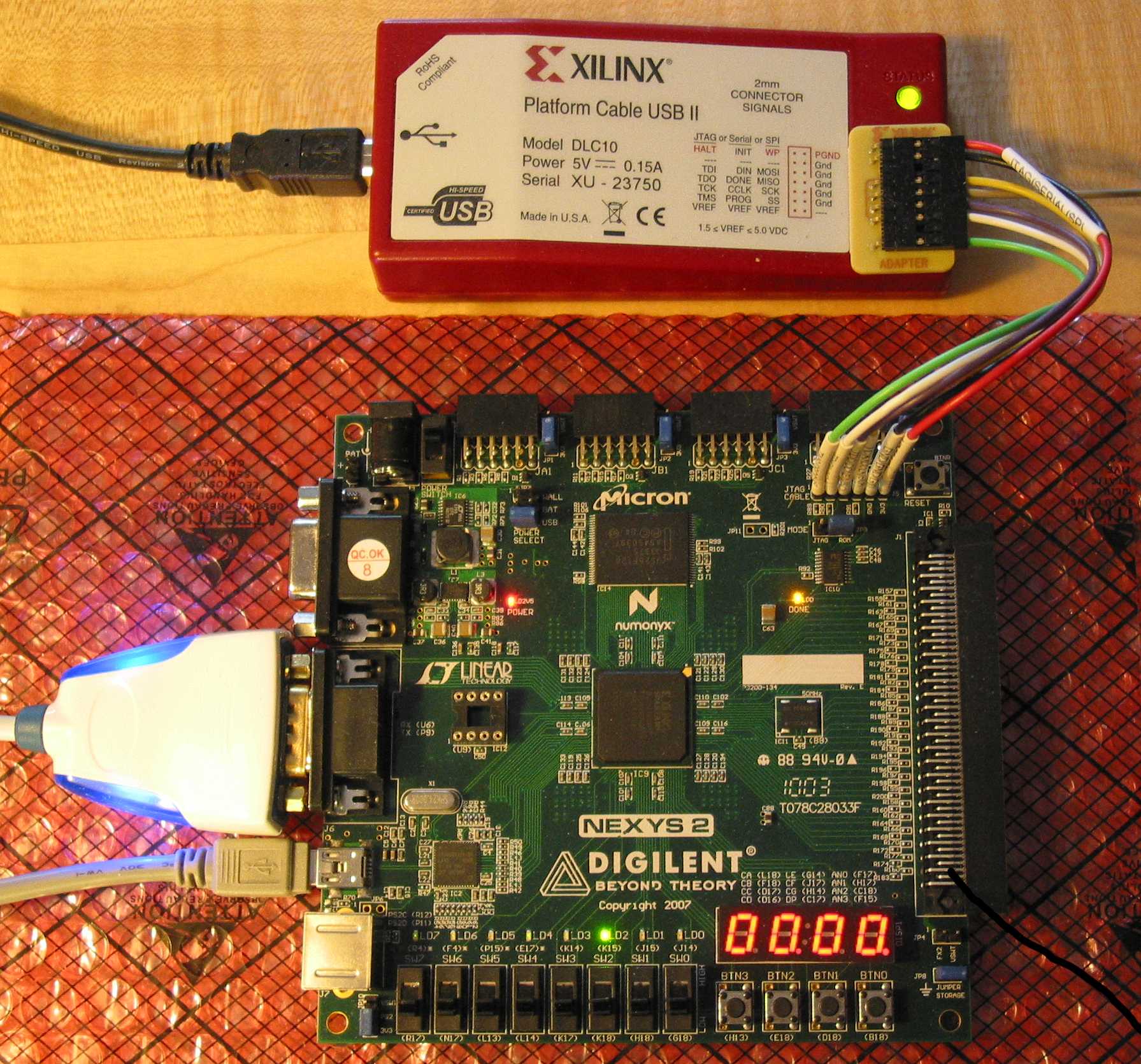
- in the current implementation the backend server is a process running on a normal Linux system. The communication is done over a rlink over high speed USB FIFO channels. See Figure F-3 for such a setup.
Currently available is a basic set of UNIBUS peripherals which is, apart from the IIST, quite similar to a full configuration of the early 80ties:
- KW11P: programmable clock
- KW11L: line frequency clock
- DL11: console interface
- DZ11: 8 lines serial port multiplexer
- LP11: line printer
- PC11: paper tape reader/puncher
- DEUNA: Ethernet interface
- RK11: disk controller with 8 RK05 drives (2.4 MByte capacity each)
- RL11: disk controller with 4 RL02 or RL01 drives (10 or 5 MByte capacity each)
- RH70: massbus adaptor with 4 RP or RM drives (with 66 to 504 MByte capacity each)
- TM11: tape controller with 4 TU10 drives
- IIST: interprocessor interrupt and sanity timer (operationally not used so far, but was fun to do...)
Complete Systems
The project holds all the sources to synthesize a complete system. The systems are comprised of
- w11a processor core
- I/O subsystem
- cache subsystem: 8-128 kByte, 32 bit cache line, fully associative, write-thru
- memory subsystem interface with PDP-11/70 style control registers
- memory controller: depends on board, currently for SRAM, PSRAM, and SDRAM (via Xilinx MIG core)
- rlink interface: used as control and debug interface as well as for I/O emulation
Complete configurations for nine boards are currently part of the project, six are FPGA verified, one is only simulation verified:
  Name              Board       FPGA      Clk   Mem  --- Resource Usage --- Veri
                                          MHz    kB   flop  luts  slices
  sys_w11a_c7       Cmod A7     XC7A35T    80   672   3411  6468  2021(25%) FPGA
  sys_w11a_as7      Arty S7     XC7S50     75  3840   6843 10040  3184(39%) sim
  sys_w11a_arty     Arty A7     XC7A35T    72  3840   6842 10090  3210(39%) FPGA
  sys_w11a_b3       Basys3      XC7A35T    80   176   3011  5936  1906(23%) FPGA
  sys_w11a_n4d      Nexys A7    XC7A100T   80  3840   6805  9830  3282(21%) FPGA
  sys_w11a_n4       Nexys4      XC7A100T   80  3840   3455  6416  2100(13%) Note 1
  sys_w11a_n3       Nexys3      XC6SLX16   64  3840   3167  6336  2141(93%) FPGA
  sys_w11a_n2       Nexys2      XC3S1200E  52  3840   3220  9948  5846(67%) FPGA
  sys_w11a_s3       S3board     XC3S1000   50  1024   3020  9388  5589(72%) Note 2

  legacy BRAM only versions
  sys_w11a_br_as7   Arty S7     XC7S50     80   256   2891  5842  1862(23%) sim
  sys_w11a_br_arty  Arty A7     XC7A35T    80   176   2891  5808  1834(23%) FPGA
  sys_w11a_br_n4d   Nexys A7    XC7A100T   80   512   3099  6109  1957(12%) FPGA

  Notes:
    Note 1: Board failed in July 2019. FPGA tested before, since then only sim tested
    Note 2: Board available but effectively retired
The Digilent Nexys2, Nexys3, and Nexys4 boards have 16 MByte PSRAM (mt45w8mw16b) of which only 4 MByte, the maximum a PDP-11 can address, are used. The Digilent Cmod A7 has a 512 kByte SRAM (is61lv25616), which is extended by 160 kByte from BRAM. The Digilent S3board has 1 MByte SRAM (is61lv2561). The Digilent Basys3 has no memory external to the FPGA. The memory seen by the w11a core is built from BRAMs, with a total size of 176 kB. The DDR memory on the Digilent Arty A7, Arty S7, and Nexys A7 is now supported. In addition, designs that use only the BRAMs are provided and offer limited memory visible to the w11a core.
System Configuration
All systems have the following configuration for the UNIBUS peripherals:
  Controller Name                    CSR  VEC PRI    Device Names
                                                     BSD     DEC
  IIST    MP interrupt/timer      177500  260  6     -       -         optional
  KW11-P  programmable clock      172540  104  6     -       -
  KW11-L  line frequency clock    177546  100  6     -       -
  RL11    disk controller         174400  160  5     rlxh    DLx:      (x=0..3)
  RK11    disk controller         177400  220  5     rkxh    DKx:      (x=0..7)
  RH/RP   disk controller         176700  254  5     xpxa    DBx:,DRx: (x=0..3)
  TM11    tape controller         172520  224  5     mt      MTx:      (x=0..3)
  DEUNA   ethernet interface      174510  120  5     de 0    XE0:
  DL11    console                 177560  060  4     cn 0    YL0:
  DL11    2nd console             176500  300  4     ttyl 1  YL1:
  DZ11    terminal interface      160100  310  5     tty *   YZx:      (x=0..7)
  PC11    papertape read/punch    177550  070  4     -       PP:,PR:
  LP11    line printer            177514  200  4     lp 0    LP:

  devices yet to be implemented:
  CR11    card reader             177160  230  6     -       CR:
  DU11    synchronous interface   160120  320  5     -       XU: